 By Adri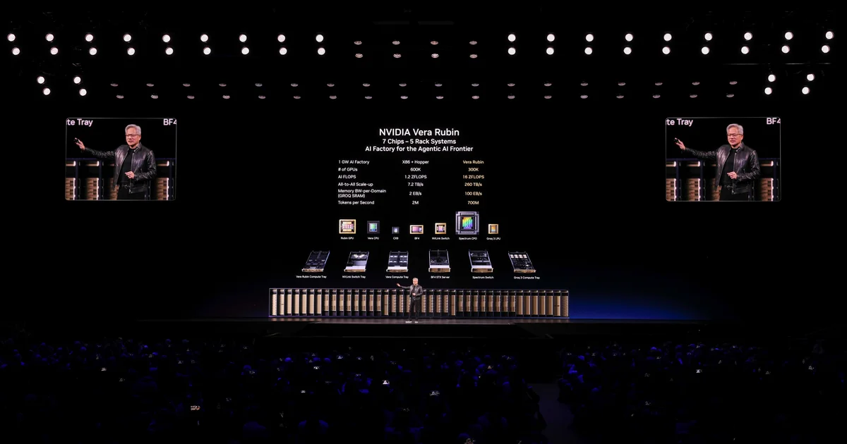
Three or four years. That is roughly the window Jensen Huang gave China during an All-In Podcast interview when discussing the country's ability to develop advanced semiconductor manufacturing equipment domestically.
Huang's argument is less about one particular prototype than China's industrial capacity. The country combines enormous manufacturing scale, semiconductor investment and a strong incentive to replace foreign equipment that is increasingly difficult to obtain. From that perspective, he sees continued progress as a matter of time.
The word “advanced” is doing a lot of work
Lithography is not a single technological threshold. China's domestic suppliers have already been working toward increasingly capable deep-ultraviolet equipment, and Reuters reported further progress around homegrown immersion DUV systems this year.
That matters. Better DUV tools, paired with increasingly complex multi-patterning processes, could expand what Chinese fabs can manufacture without immediately reproducing the most sophisticated machines available in Europe.
EUV is a different problem.
ASML remains effectively alone in commercial extreme-ultraviolet lithography, a technology built from an unusually difficult combination of precision optics, light sources, motion systems, metrology and a specialized supplier network assembled over decades.
The target is also moving. Major chipmakers are now preparing broader adoption of ASML's High-NA EUV systems. Those machines cost roughly $400 million and are designed to print features substantially smaller than today's mainstream EUV platforms.
A prototype would only be the beginning
Semiconductor manufacturing makes impressive demonstrations look almost easy compared with mass production. A lithography system intended for a fab must repeatedly expose wafers with extremely tight alignment while maintaining useful throughput, reliability and acceptable operating costs.
That distinction is important when evaluating Huang's 2030 prediction. China could unveil a genuinely advanced domestic lithography platform before the end of the decade and still remain behind ASML in production capability.
A capable immersion DUV machine would already have strategic value. A production-ready EUV system competitive with ASML would represent a much larger technological jump. The original prediction does not clearly establish which of those outcomes Huang considers sufficient.
Huang has a particularly close view of the bottleneck
This is not an abstract subject for NVIDIA. Modern AI accelerators depend on cutting-edge foundry processes, advanced packaging, high-bandwidth memory and an increasingly complicated manufacturing chain. More compute cannot simply appear because a GPU architecture looks good on a slide.
Huang has also repeatedly expressed confidence in the speed of Chinese engineering and manufacturing development. That gives the comment useful industry context, but it does not make 2030 a confirmed semiconductor roadmap.
Current market conditions remain heavily tilted toward ASML. The Dutch manufacturer still controls almost all leading-edge lithography and has no commercial peer offering EUV equipment at comparable maturity. Chinese suppliers are advancing from much further back.
The factory floor will decide
The meaningful milestone will not be a press conference or a laboratory machine. It will be several systems operating inside fabs, processing wafers at useful volume with repeatable results.
If that happens by 2030, Huang's prediction will have aged remarkably well. Until then, the date is best read as an aggressive assessment of China's industrial trajectory rather than proof that an ASML-class machine is four years away.