
 By Adri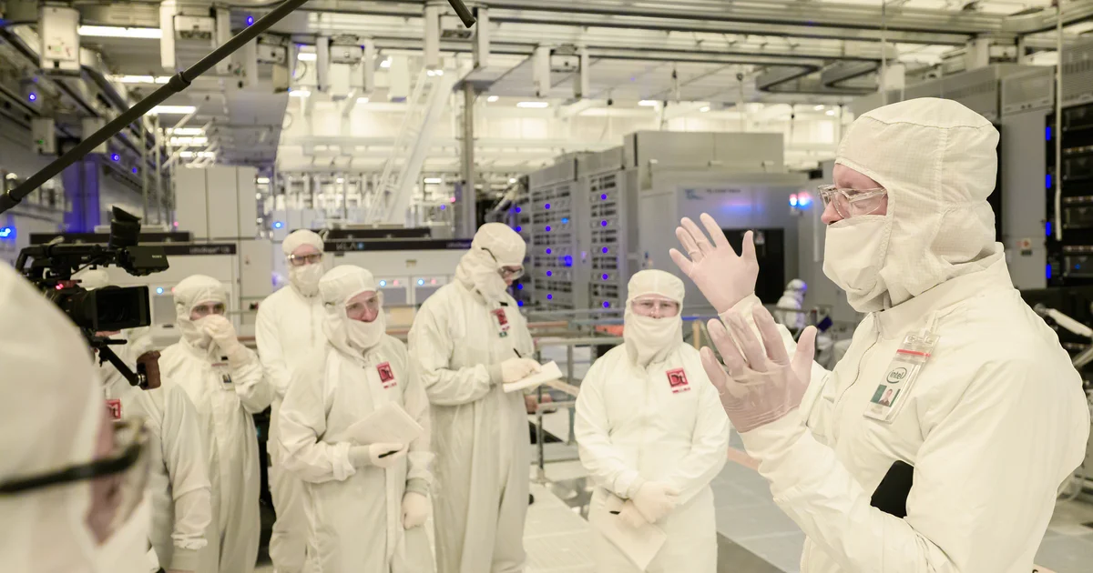
High-NA EUV has moved well beyond a laboratory demonstration in 2026. Intel is already using it on selected Intel 18A production layers, while TSMC, Samsung and SK Hynix are all moving toward their own deployment strategies.
Reuters now describes much broader industry alignment around ASML's next-generation platform than existed when the first tools shipped. The price remains extraordinary: High-NA systems are generally valued at roughly $350 million to $400 million depending on generation and configuration.
The reason that number can still make economic sense is that the competing approach often means sending the wafer through additional lithography steps.
Going from 0.33 to 0.55 directly changes resolution
High-NA does not use a shorter wavelength than conventional EUV. Both generations still operate with 13.5nm extreme-ultraviolet light.
The major change is numerical aperture. NXE scanners use 0.33 NA optics. ASML's EXE platform moves to 0.55 through an extensively redesigned optical system developed with ZEISS.
ASML specifies 8nm resolution for EXE:5200B, versus roughly 13nm for its NXE platform. It says High-NA can print features 1.7 times smaller in a single exposure, theoretically enabling up to 2.9 times the transistor density from geometric scaling.
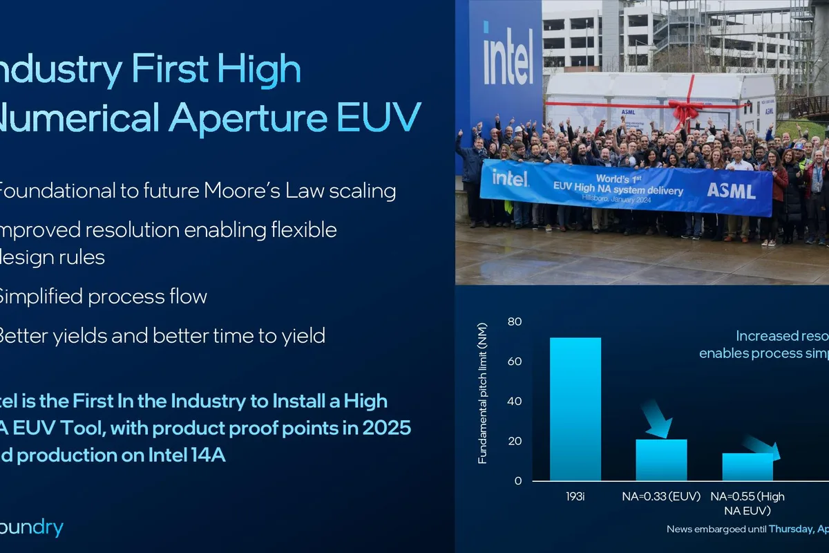
That 8nm figure should not be confused with a commercial process-node name. Lithographic resolution describes printable feature dimensions in this context; labels such as 2nm, 18A and 14A describe much broader manufacturing platforms.
The real competitor to High-NA is often another exposure
When a feature becomes too small for a clean single exposure, chipmakers can divide its patterning across multiple lithography and processing steps.
That extends the usefulness of existing scanners, but it also adds masks, alignment operations, deposition, etch, inspection and manufacturing time.
Every additional patterning step introduces another chance for variation or overlay error to reduce yield.
High-NA therefore does not have to be cheaper than Low-NA as a machine. It has to be economically preferable to the extra process complexity it can remove from the hardest layers.
Intel has already processed more than one million High-NA wafers
Intel remains the industry's most experienced early adopter. Intel and ASML said in September that more than one million wafers had now been processed on Intel's High-NA equipment.
That total includes installation, certification, R&D and production activity, so it does not mean one million commercial wafers were entirely manufactured using High-NA.
The more important milestone is that selected layers for a subset of Core Ultra Series 3, code-named Panther Lake, are already being manufactured on Intel 18A using the technology.
Those layers are dual-qualified. Intel can pattern them with High-NA EXE equipment or conventional 0.33 NA NXE scanners, and the company says the resulting performance and yields meet or exceed its comparable NXE process.
That gives Intel a conservative way to introduce an expensive new production platform without making an entire product flow immediately dependent on it.
A 150-ton scanner does not arrive as a simple fab upgrade
The physical scale helps explain the cost.
Early High-NA installations weigh well over one hundred metric tons and arrive across hundreds of crates and dozens of shipping containers. Intel's first EXE installation required months of assembly and calibration.
The architecture is modular. EUV source, projection optics, reticle system, wafer stage and other modules are transported separately and brought together inside the fab.
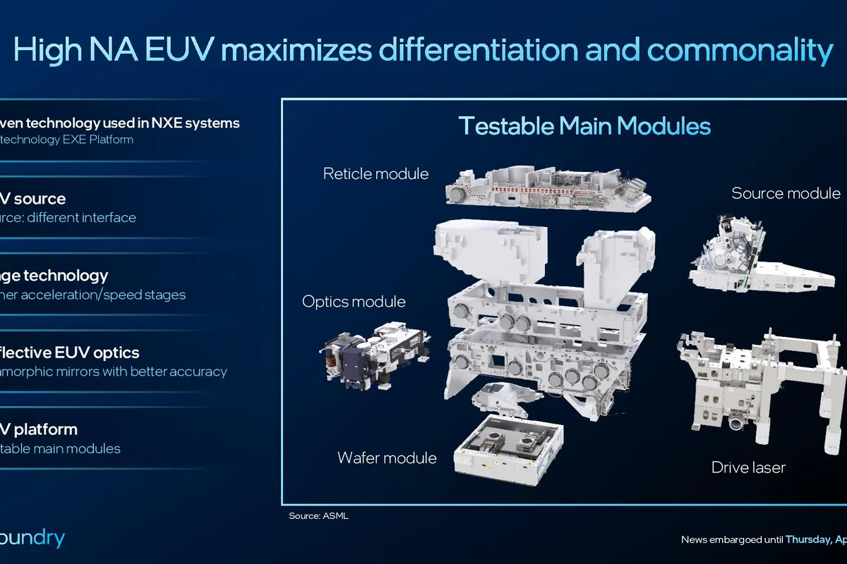
Installing one is therefore not equivalent to rolling out an older scanner and connecting a new model in the same footprint. Building structure, vibration control, power, cooling, logistics and service access all have to accommodate the platform.
EXE:5200B is about making High-NA economically manufacturable
EXE:5000 was primarily a development platform. EXE:5200B is the generation intended for volume manufacturing.
ASML specifies 0.55 NA optics, 8nm resolution and throughput of at least 175 wafers per hour at a 50 mJ/cm² exposure dose. Overlay and system availability have also been improved.
Throughput matters because extraordinary resolution is of limited value if each wafer becomes prohibitively expensive to expose.
High-NA also introduces a smaller exposure field because of its anamorphic optical architecture. Larger dies can therefore require stitching or layout strategies specifically designed around the half-field format.
TSMC does not have to follow Intel's adoption schedule
The industry is converging on the technology without converging on one timetable.
TSMC and ASML say TSMC intends to use High-NA in high-volume manufacturing for advanced nodes beginning in 2030.
Until then, TSMC can continue extracting value from existing EUV equipment and introduce High-NA only where its process economics justify the transition.
That is not the same as rejecting the technology. A modern process already mixes multiple lithography generations: the most advanced scanner is reserved for the layers that actually need it.
Samsung brings advanced DRAM into the High-NA story
Samsung has expanded its own High-NA collaboration with ASML and plans future adoption for advanced DRAM production.
That matters because EXE is not just a machine for future logic processors and GPUs.
Memory structures are becoming dense enough to benefit from its resolution at the same time that HBM and AI-server demand are pushing DRAM manufacturers toward enormous new investments.
SK Hynix is also among the memory companies building experience around High-NA as future generations become harder to pattern with existing tools.
Eventually even the photomask has to get larger
High-NA creates another infrastructure problem that rarely appears on a processor specification sheet: the mask.
Current EXE production works with the industry's established 6-inch mask format. Because High-NA exposes a smaller field, large designs may require field stitching.
TSMC and ASML have now launched an industry initiative around a larger 12-inch mask format. Their stated target is a pilot line in 2031 and broader manufacturing readiness around 2033.
That timeline shows how deep the transition runs. Buying the scanner is only one piece. Masks, EDA software, resists, metrology and design rules all have to evolve around it.
ASML can charge extraordinary prices because the alternatives are limited
ASML's commercial position remains unusual even by semiconductor-industry standards.
There is currently no competing commercial platform equivalent to its leading-edge EUV systems. Reuters estimated ASML held about 94% of the overall lithography market in 2025, with its position effectively unmatched at the most advanced EUV end.
That leaves leading foundries negotiating less about whether an equivalent alternative exists and more about when the cost of adopting ASML's next platform becomes justified.
ASML still has its own constraint: manufacturing enough scanners. Demand has pushed the company to expand EUV production capacity, with substantial additional output planned through 2027 and 2028.
High-NA costs a fortune because the alternative can cost even more
That is ultimately the business case.
An EXE scanner approaching $400 million looks extravagant when treated as a standalone piece of machinery. A leading-edge fab instead measures process steps, cycle time, overlay risk, yield and good dies per wafer.
If one High-NA exposure replaces several Low-NA-related patterning operations on a critical layer, the purchase price of the scanner becomes only one part of the equation.
Intel is already testing that proposition in production. TSMC is taking a slower path. Samsung and SK Hynix are extending the same discussion into advanced memory.
High-NA is not winning because $400 million suddenly became cheap. It is winning because, at the dimensions the industry still wants to manufacture, the alternatives are becoming extraordinarily expensive too.