
 By Adri
Kioxia and Sandisk have announced plans to invest more than $31 billion, approximately 5 trillion yen, in Japan through 2032.
The figure does not describe one factory. It covers production expansion, technology investment and related infrastructure around their major Yokkaichi and Kitakami manufacturing sites.
Both companies explicitly say the program is contingent on Japanese government support.
That condition matters. Building advanced NAND capacity now requires billions of dollars long before the first commercially useful wafers leave the line.
Fab3 is planned directly south of Fab2
The most visible project is a new Fab3 at Kioxia's Kitakami Plant in Iwate Prefecture.
Kioxia says site preparation is already underway. The building will sit south of Fab2 and is targeted to begin operations during fiscal 2029.
The company has not yet fixed every construction milestone or final equipment purchase.
Those details will be adjusted according to market conditions.
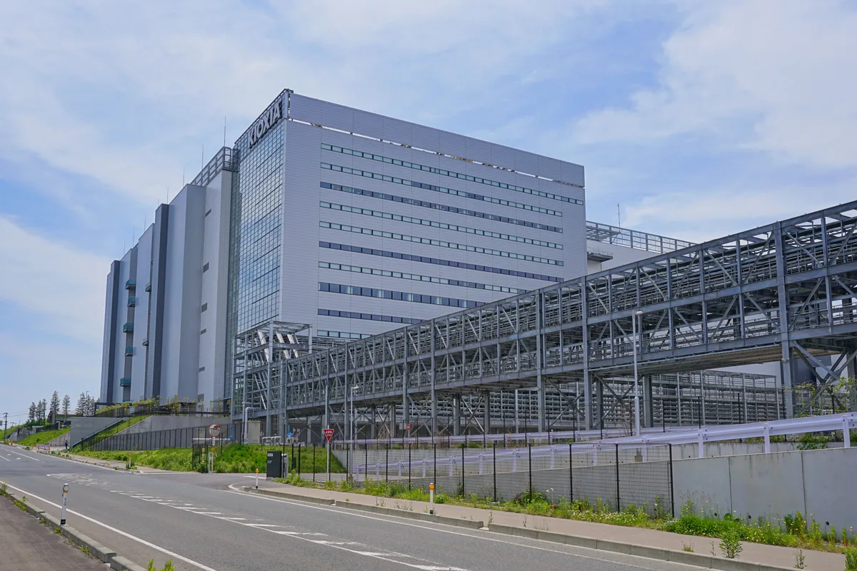
Reuters reports that Kioxia expects roughly 1.8 trillion yen of investment for the new facility, equivalent to about $11.3 billion using the exchange rate cited when the announcement was made.
Fab3 could therefore absorb more than one-third of the total capital program by itself.
Kitakami's second fab has barely started operating
The timing is striking because Fab2 is not an aging plant already due for replacement.
K2 began operating in September 2025.
Kioxia and Sandisk started producing their tenth-generation 3D flash technology there in July 2026.
That BiCS FLASH generation uses technologies including CMOS directly bonded to the memory array and targets higher density, stronger performance and lower power.
For its tenth-generation TLC devices, Kioxia specifies NAND interface speeds up to 4.8 Gb/s, 33% above its eighth-generation technology.
Preparing K3 while K2 is still scaling therefore shows that the company is already planning for the next manufacturing cycle.
The investment is not simply about constructing more buildings
Semiconductor factories do not gain capacity only by adding square meters.
A major portion of NAND bit growth comes from the memory technology itself.
Greater vertical density allows more storage to be produced from a given silicon area. Better yields, faster interfaces and manufacturing improvements also increase useful output from existing infrastructure.
The $31 billion program therefore spans physical expansion, manufacturing equipment, process technology and further buildout inside current sites.
That matters because twice the capital expenditure does not automatically mean twice the number of wafers.
Why does AI need this much NAND in the first place?
The first answer is datasets.
Models are trained on enormous collections of text, images, video, code and structured data. Once training is complete, inference infrastructure still produces and consumes caches, embeddings, vector databases, checkpoints, logs and generated content.
That material cannot all remain in HBM.
HBM is extraordinarily fast and extraordinarily expensive. Server DRAM offers much more capacity, but it is still far too costly to function as permanent storage at data-center scale.
NAND takes over as soon as information needs to remain readily accessible without requiring memory-class latency.
Inference changes the storage profile even more
Training concentrates enormous compute demand into a finite project.
Inference turns the resulting model into a persistent service.
Thousands or millions of requests can access different documents, retain context, query retrieval systems and interact with agentic workflows.
Kioxia explicitly names agentic AI, physical AI and on-device AI as long-term drivers of flash demand.
All three increase the amount of information created and accessed around the model rather than merely increasing matrix operations on a GPU.
An AI agent can create a much heavier storage footprint than a chatbot
A conventional chatbot primarily responds to a sequence of prompts.
An agent can maintain working memory, read documents, generate files, query databases, invoke tools and retain records of those actions.
Multiply that behavior across thousands of enterprise agents and the storage profile starts looking very different from a simple text-generation API.
SSDs do not replace GPU memory. They become the massive tier that keeps everything else from falling much farther down into slower storage.
Kioxia is already designing SSDs around this new hierarchy
The company is not merely trying to manufacture more raw NAND bits.
Its recent products show how it expects those bits to be used.
GP1, for example, targets up to 10 million random-read IOPS and is designed for GPU-initiated access in AI infrastructure.
Kioxia is also pushing PCIe 6.0 enterprise SSDs, CXL-compatible memory expansion and E1.S products for hyperscale systems.
The direction is consistent: as HBM and DRAM become too expensive to contain the entire working set, flash is being pulled much closer to compute.
Sandisk and Kioxia are separate companies, but they have manufactured together for more than twenty-five years
The joint nature of the investment can look unusual now that Sandisk is again operating as an independent company.
The manufacturing relationship is much older.
Kioxia and Sandisk have jointly developed and produced NAND wafers in Japan for more than twenty-five years.
The companies say they have invested more than $50 billion, approximately 9 trillion yen, in Japan over that period.
In January 2026 they extended their Yokkaichi joint-venture framework through the end of 2034. The Kitakami arrangement is aligned with the same horizon.
The resulting chips can end up in different commercial products, but a fundamental portion of their manufacturing investment is shared.
That shared capital is particularly useful in a brutally cyclical market
NAND has a long history of painful boom-and-bust cycles.
If every manufacturer builds too much capacity at once, oversupply can crush prices.
If investment is held back for too long, demand can outrun supply and push pricing sharply in the opposite direction.
A fab takes years to build, making it impossible to respond cleanly to swings that last only a few quarters.
Kioxia and Sandisk are therefore making decisions now about capacity that may not begin producing until around 2029.
Their bet is not that the market stays strong this winter. It is that the flash market is structurally much larger at the start of the next decade.
The Japanese government is part of the financing equation
The companies repeatedly state that the announced investments depend on government support.
Japan has already subsidized Kioxia and Sandisk expansion as part of a broader policy to rebuild domestic semiconductor capacity.
That strategy includes memory, advanced logic, packaging and semiconductor materials.
The objective therefore extends beyond Kioxia's individual profitability. Japan wants to retain domestic production capacity in a sector whose supply chains are highly concentrated across Asia.
For Kioxia and Sandisk, public support reduces part of the financial risk attached to assets whose payback takes many years.
NAND is not HBM, and that is exactly why it matters
AI memory discussions often stop at HBM because it sits physically beside the industry's most expensive accelerators.
The rest of the infrastructure forms a much broader pyramid.
Hundreds of gigabytes of HBM can sit above terabytes of DRAM and tens or hundreds of terabytes of flash before data moves into still larger object-storage and archival tiers.
Kioxia and Sandisk are investing lower in that pyramid, where cost per gigabyte matters far more than absolute latency.
As models and datasets expand, the base has to widen too.
More than $31 billion does not mean every dollar is already committed
The announcement still needs to be read cautiously.
The companies describe anticipated investments through 2032, contingent on government support and adaptable to market conditions.
Kioxia explicitly says detailed Fab3 construction timing and production-equipment investment will be determined according to demand.
The figure is therefore a capital roadmap rather than a purchase order already issued to every equipment supplier.
A prolonged NAND downturn could slow parts of the rollout. Stronger-than-expected AI demand could push equipment installation in the opposite direction.
The AI race eventually turns into a race for cleanroom floor space
AI announcements usually talk about models, GPUs and tokens per second.
A few layers deeper into the supply chain, those same trends become much more physical.
Companies have to acquire land, construct cleanrooms, order manufacturing tools, secure power and water, improve yields and then wait for each generation to reach acceptable production maturity.
Fab3 is targeted to begin operating in 2029 even though site preparation started in 2026.
That delay is what makes the Kioxia-Sandisk plan significant.
The companies are not merely responding to today's demand. They are committing tens of billions of dollars to the assumption that six years from now, the AI economy will still need far more places to store everything it computes.