
 By Adri
Samsung Electronics and ASML expanded their semiconductor-manufacturing partnership on September 8.
The agreement contains two related projects operating on very different timelines.
Samsung intends to introduce ASML High-NA EUV into future DRAM high-volume manufacturing by 2028.
It is also joining the industry initiative developing 12-inch photomasks for a later generation of High-NA production.
The first project does not depend on the second being ready.
High-NA changes the optics, not the EUV wavelength
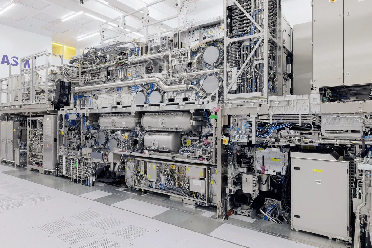
ASML's established NXE scanners and its newer EXE systems both use 13.5nm extreme-ultraviolet light.
The major optical change is numerical aperture.
NXE systems operate at 0.33 NA. The EXE High-NA platform raises that to 0.55.
A higher numerical aperture allows the projection system to resolve finer detail on the wafer.
ASML specifies roughly 8nm resolution for the EXE platform compared with about 13nm for its conventional EUV generation.
DRAM is particularly unforgiving when structures stop shrinking cleanly
A modern DRAM device repeats enormous numbers of memory cells built around structures including a transistor and capacitor.
Each generation tries to reduce cell area while maintaining electrical behavior and manufacturing yield.
Once a lithography tool can no longer resolve a required pattern directly, engineers compensate with additional patterning operations.
A feature can be divided across multiple exposures with deposition, etch and alignment steps inserted between them.
Those extra operations consume fab time and create more opportunities for defects.
Samsung already has years of EUV DRAM experience
High-NA will not be Samsung's first use of EUV in memory.
In 2020, the company announced shipment of one million DDR4 modules using its first EUV-patterned 10nm-class D1x DRAM.
Later memory generations expanded EUV use to additional layers.
The 2028 plan is therefore better understood as the next optical generation of an established manufacturing strategy rather than Samsung's first move away from DUV.
Higher resolution can eliminate process complexity
ASML's main economic argument for High-NA is not simply that it prints a smaller line.
If one exposure can replace a more complicated multi-patterning sequence, several associated process steps may disappear with it.
Fewer exposures can also mean fewer alignment operations, etches, depositions and inspections.
That can shorten cycle time and reduce opportunities for defect introduction.
Samsung has not yet published a quantified cost or yield improvement for its future High-NA DRAM process.
High-NA also introduces a field-size compromise
Increasing NA required substantially different mirrors.
ASML avoided forcing the semiconductor industry to replace its entire mask ecosystem immediately by using anamorphic optics.
The EXE system demagnifies the mask pattern by four times in one direction and eight times in the other.
That allows conventional six-inch reticles to remain usable.
The tradeoff is a smaller exposure field.
Large designs may therefore need stitching
With today's mask format, some structures larger than the High-NA half-field have to be divided between exposures.
Those portions are then stitched together on the wafer.
The approach works, but the boundary has to meet demanding overlay tolerances.
A production process therefore inherits another alignment problem that did not exist in the same form with a full-field conventional EUV exposure.
Intel and ASML are already presenting manufacturing work specifically focused on High-NA reticle stitching.
A 12-inch mask tries to remove the need for that workaround
The semiconductor industry has relied on six-inch photomasks for decades.
The initiative Samsung is joining aims to double that format to 12 inches.
A larger mask can carry a correspondingly larger pattern field for a future High-NA scanner architecture.
ASML and Samsung say the transition is expected to improve fab productivity, lower manufacturing cost and remove stitching constraints.
Those are objectives for a future platform, not characteristics of Samsung's current production tools.
A bigger photomask requires a new ecosystem around it
An EUV reticle is not simply an oversized photographic plate.
It is a multilayer reflective optical component carrying the circuit pattern used by the scanner.
Changing its dimensions affects mask blanks, pattern writing, inspection, defect repair, transport, storage and precision handling inside lithography equipment.
Metrology tools and standards have to evolve too.
That is why changing the mask format is an industry program rather than something ASML or Samsung can implement alone.
The timing shows how large that transition really is
ASML and TSMC launched the broader large-format mask initiative on September 7, one day before Samsung announced that it was joining.
The program targets a 12-inch photomask pilot line in 2031.
It aims for advanced-node lithography-system readiness around 2033.
Samsung's DRAM target arrives roughly five years earlier.
Its first High-NA memory manufacturing therefore remains compatible with today's six-inch mask ecosystem.
High-NA itself has already moved beyond laboratory demonstrations
Intel Foundry said in September that High-NA is already being used on selected layers for a subset of Core Ultra Series 3 processors manufactured on Intel 18A.
Intel reports more than one million wafers processed across early tool certification, R&D and volume production on selected layers.
That does not mean every Intel 18A layer uses High-NA.
Advanced lithography tools are deployed where their resolution or process simplification provides enough benefit to justify them.
Samsung is targeting a different milestone: volume DRAM
Samsung and ASML describe the 2028 plan as the industry's first intended use of High-NA in DRAM high-volume manufacturing.
That remains a manufacturing roadmap commitment rather than a finished process.
Samsung has not identified the commercial DRAM generation, number of High-NA layers or exact EXE scanner configuration that will be used.
Those choices will follow process-development results.
Not every layer needs the most advanced scanner
A semiconductor contains layers with very different resolution requirements.
The densest patterns may justify High-NA.
Other layers can remain on 0.33-NA EUV or even DUV equipment.
Using the most expensive lithography platform for patterns that do not require it would increase manufacturing cost without adding value.
Samsung therefore has to identify the layers where fewer process steps or tighter resolution produce a clear economic return.
ASML's 8nm resolution is not an 8nm process node
The two concepts are easy to confuse.
Modern node names are no longer direct measurements of one transistor dimension.
An 8nm optical-resolution specification for EXE therefore does not mean Samsung's future DRAM uses a manufacturing process called 8nm.
It describes the lithography platform's ability to resolve fine structures.
Half-field optics also forced ASML to make the stages much faster
A reduced exposure field means more exposures are required to cover a wafer.
ASML compensated by substantially increasing wafer-stage and reticle-stage acceleration.
For the EXE:5000, the company has described an 8g wafer stage and a reticle stage reaching 32g.
The system has to maintain nanometer-class precision while those stages move at extraordinary speed.
Resolution alone would be commercially useless if wafer throughput collapsed.
Memory economics ultimately come down to cost per bit
A DRAM generation can be technologically advanced and still fail economically if each bit is too expensive to manufacture.
Memory makers therefore need density, yield and process simplicity to improve together.
High-NA may improve resolution while removing some multi-patterning sequences.
The equipment itself is also extremely expensive.
The business case depends on using it only where the eliminated process complexity offsets that additional capital cost.
The 12-inch photomask belongs to the second phase of that economic equation
ASML designed the first EXE generation to enter fabs without requiring a simultaneous replacement of the existing mask infrastructure.
That reduced the number of technologies the industry had to reinvent at once.
Large-format masks come later.
If the ecosystem succeeds, future High-NA systems could recover more usable exposure field and eliminate some stitching overhead.
The improvement would then concern not only printable dimensions but also wafer-level manufacturing efficiency.
Samsung is positioning itself on both timelines
One target is relatively near: High-NA DRAM production by 2028.
The other reaches into the early 2030s, when the mask ecosystem itself may be ready to move beyond the six-inch format.
That combination makes sense for a company operating both memory fabs and an advanced logic foundry.
A future 12-inch mask platform would not be limited to DRAM.
It could also matter for increasingly large and complex logic designs where half-field stitching becomes a meaningful manufacturing constraint.
Memory is becoming one of High-NA's first major industrial proving grounds
EUV was initially associated most visibly with cutting-edge logic processors.
Samsung brought it into DRAM relatively early.
Six years after its first million EUV DRAM modules, the company is now preparing the next generation of EUV optics for memory production.
The 2028 date remains a target rather than an accomplished deployment.
It nevertheless shows that High-NA is moving beyond a technology demonstrated for extreme logic scaling.
And the 12-inch mask initiative reveals what happens next: once the scanner wins more resolution, the rest of the lithography ecosystem has to catch up before that resolution can be used with fewer compromises.