
 By Adri
Samsung Electronics and ASML announced an expansion of their lithography partnership on September 8.
The nearer-term part of the agreement concerns memory manufacturing.
Samsung plans to introduce High-NA EUV into high-volume production of future DRAM by 2028.
Samsung and ASML describe that as the first planned High-NA deployment in DRAM production.
High-NA changes the optics before it changes the light source
Conventional EUV and High-NA EUV both use 13.5nm extreme-ultraviolet light.
The major change is the numerical aperture of the projection optics.
Today's NXE production platform operates at 0.33 NA.
ASML's EXE generation raises that figure to 0.55.
ASML specifies 8nm resolution for the High-NA platform, compared with roughly 13nm for its 0.33 NA EUV systems.
The company says an EXE:5000 can print features 1.7 times smaller in a single exposure than the NXE generation.
Those are lithography-system specifications. They are not direct statements about the marketed node name or physical size of a future Samsung DRAM cell.
For DRAM, better resolution can mean fewer patterning steps
When a feature becomes too small for one clean exposure, chipmakers can split the job across multiple patterning steps.
That introduces additional deposition, etch, alignment and inspection operations.
Every added operation lengthens cycle time and creates another opportunity for overlay error or process defects.
High-NA's higher resolution can return some layers to simpler exposure flows.
Samsung and ASML explicitly cite process simplification and efficiency as reasons the technology can extend the DRAM scaling roadmap.
Memory has already gone through one EUV transition
Samsung is not approaching High-NA without production experience in EUV.
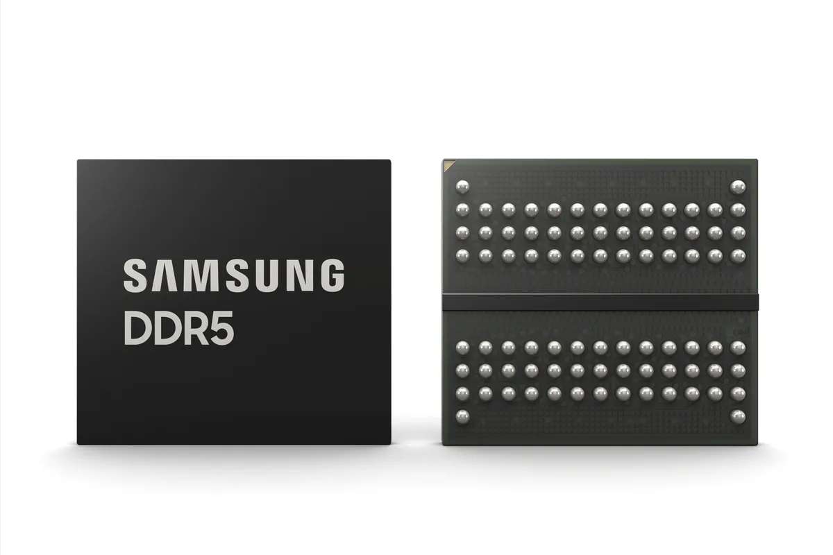
The company shipped its first EUV-based DRAM in 2020 and announced mass production of 14nm DDR5 using five EUV layers in 2021.
Moving to 0.55 NA is a different step.
Rather than progressively replacing complicated DUV patterning with standard EUV, the scanner's own imaging resolution is now being increased.
Why is shrinking DRAM becoming so difficult?
A DRAM cell is conceptually simple: a transistor controls access to charge stored in a capacitor.
Manufacturing billions of those cells with extremely consistent dimensions is not.
Shrinking line and contact pitch while preserving sufficient electrical behavior, capacitance, reliability and yield pushes lithography closer to its limits.
Overlay margins become tighter as structures shrink as well.
Higher-resolution lithography does not solve capacitor scaling, materials or every cell-architecture problem, but it can remove some of the pressure from patterning.
High-NA can also shorten the process flow
ASML presents process simplification as one of the main economic arguments for its EXE platform.
Reducing double or multiple patterning can remove operations from a critical layer.
Fewer operations can shorten cycle time and reduce the number of process steps capable of creating defects.
Samsung similarly says High-NA should improve manufacturing efficiency while extending memory scaling.
Neither company has published a quantified yield or cost improvement for Samsung's planned 2028 DRAM implementation.
High-NA tools are already operating in industry
The platform is no longer confined to a research demonstration.
ASML shipped the first High-NA system at the end of 2023.
EXE tools have since moved into early industrial use.
Intel Foundry said in September 2026 that more than one million wafers had already passed through High-NA systems across tool qualification, R&D and volume manufacturing on selected layers of a subset of Panther Lake processors.
Samsung's memory timetable therefore follows the pattern ASML has described for years: leading logic first, followed by memory at a similar density requirement.
The second project concerns something much older: the photomask
Samsung is also joining the industry initiative to develop a 12-inch photomask platform.
A photomask carries the pattern a lithography system ultimately projects onto a wafer.
The semiconductor industry has used the current roughly 6-inch format for decades.
The scanner surrounding that mask has changed radically while the reticle format has largely remained constant.
The first High-NA systems were deliberately designed to keep using 6-inch masks
That is crucial to understanding the timeline.
ASML's first EXE systems use anamorphic projection optics.
The image is treated differently across the two axes, allowing High-NA to preserve the established reticle format despite the much larger mirrors required for 0.55 NA.
The compromise is a field that is half-sized in one direction.
For sufficiently large patterns, multiple exposures have to be joined together.
That join is known as stitching.
The 12-inch mask is intended to remove that compromise later
A substantially larger reticle can recover more usable exposure area while preserving High-NA optical performance.
ASML expects the transition to improve scanner productivity, reduce chip-manufacturing cost and remove stitching constraints.
The main benefit is therefore not higher optical resolution from the mask itself.
It is a more efficient way to use the High-NA scanner's resolution across larger patterns.
2028 is not the date for 12-inch masks
The announcements arrived together, but their schedules are separated by several years.
Samsung plans High-NA DRAM production by 2028 using the existing mask ecosystem.
The broader ASML and TSMC large-format-mask initiative targets a 12-inch pilot line around 2031.
Full lithography-system readiness for advanced production using the larger platform is targeted around 2033.
Samsung's first High-NA DRAM therefore does not depend on 12-inch masks being available.
Changing mask size means changing an entire manufacturing ecosystem
A 12-inch transition is not a matter of manufacturing a larger plate and placing it in today's scanner.
Mask writers, inspection systems, metrology, cleaning, pellicles, robotic handling and transport infrastructure all have to support the new format.
Standards also need to define physical dimensions and interfaces across multiple suppliers.
That is why Samsung is joining an industry initiative rather than attempting to make the transition alone.
High-NA economics depend heavily on scanner productivity
A more precise lithography tool only makes sense in production if it can process enough wafers at an acceptable cost.
ASML has therefore evolved the EXE roadmap around throughput as well as imaging performance.
Its April 2026 public roadmap places the EXE:5200B at up to 175 wafers per hour under specified no-stitching conditions, with later 5200C and 5200D generations targeting higher output.
Those figures depend on exposure dose and operating conditions.
They are not guaranteed Samsung DRAM fab throughput numbers.
Stitching costs throughput because one pattern requires more scanner work
With a reduced anamorphic field, some large layouts require more than one precisely aligned exposure.
Every additional exposure consumes scanner time.
The boundary between fields also has to meet extremely tight tolerances to avoid turning the stitch into a functional defect.
Larger masks are therefore as much an economic project as a geometric one.
ASML and TSMC explicitly describe the initiative as a way to extract more productivity from future High-NA systems.
Samsung can use this work across both memory and foundry
Samsung occupies an unusual position because it manufactures its own memory while also operating a foundry for external customers.
A future 12-inch-mask ecosystem can therefore affect several classes of semiconductor.
DRAM uses highly repetitive structures and its own density constraints.
Advanced logic has increasingly complex transistor architectures and highly varied customer layouts.
The same lithography platform can be useful to both while being optimized differently in each process.
AI demand is indirectly pushing memory lithography harder
AI accelerators have sharply increased demand for advanced DRAM, particularly HBM.
HBM gains capacity and bandwidth by stacking multiple dies, but every one of those dies still has to be manufactured from a DRAM process that continues improving density and efficiency.
Three-dimensional packaging does not remove the need to advance the underlying memory process.
That is part of the connection Samsung and ASML make between High-NA development and the AI era.
High-NA alone will not decide the HBM competition
An HBM stack also depends on die yield, TSVs, bonding, thermal behavior, packaging and the logic interface.
A more advanced DRAM lithography process can improve the underlying memory generation without guaranteeing that one finished HBM product outperforms another.
Samsung's 2028 High-NA target should therefore be read as a manufacturing roadmap, not as a performance announcement for a specific future HBM generation.
Introducing High-NA into memory production brings its own qualification burden
A new scanner generation requires new work around overlay, resist, dose, mask behavior, inspection and process recipes.
Its economic advantage appears only when the reduced process complexity compensates for the cost and difficulty of introducing the tool.
Samsung has not yet identified the exact commercial DRAM generation that will receive its first High-NA layer or how many layers will use the technology.
The public commitment is to introduce High-NA into high-volume DRAM manufacturing by 2028.
This is ultimately another attempt to change the economics of scaling
Conventional EUV let the semiconductor industry continue shrinking patterns without endlessly multiplying DUV lithography steps.
High-NA extends the same strategy: accept a dramatically more complex optical system in exchange for reducing complexity elsewhere in the process.
The 12-inch photomask initiative then addresses another cost embedded in that optical design by attempting to remove stitching and increase scanner productivity.
Samsung is preparing for two different horizons.
The first is close enough to have a date: 0.55 NA lithography in DRAM high-volume manufacturing by 2028.
The second requires changing a piece of the lithography ecosystem whose physical format has survived for decades.
If the current roadmap holds, High-NA DRAM will already be in production years before the 12-inch mask platform reaches its intended industrial phase.