
 By Adri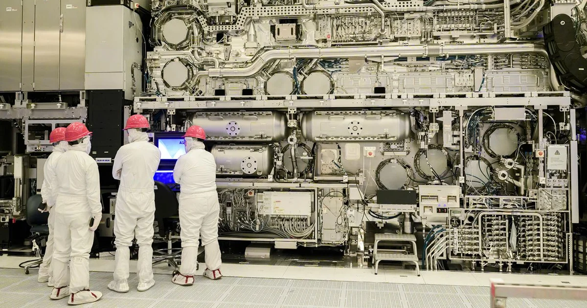
Intel Foundry and ASML have crossed the one-million-wafer mark with High Numerical Aperture EUV lithography. The number covers several types of work, including early tool certification, testing, research and development and volume manufacturing.
That qualification matters. Intel is not claiming to have manufactured one million complete Panther Lake wafers with High-NA. It is showing how much practical exposure its fabs have accumulated with a technology most of the industry is still preparing to deploy at scale.
High-NA is already touching shipping-class Panther Lake silicon
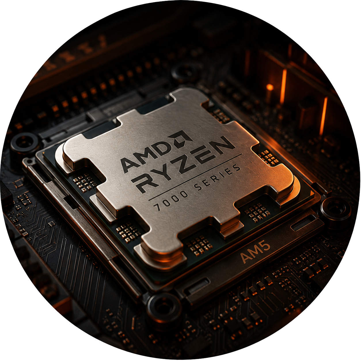
Intel says selected layers on a subset of Core Ultra Series 3 processors, better known as Panther Lake, are now patterned using High-NA EUV on the Intel 18A process.
The company says those High-NA layers meet or exceed the performance of comparable layers produced with conventional 0.33-NA NXE EUV systems. Overlay, throughput and availability are also said to be meeting Intel Foundry's expectations.
Intel is not replacing every lithography step with the newer machines. High-NA is being inserted selectively where its additional resolution provides enough value to justify the complexity and cost.
The jump from 0.33 NA to 0.55 NA comes with baggage
High-NA EUV raises numerical aperture from 0.33 to 0.55, allowing finer features to be resolved. That provides another route toward smaller transistor dimensions while potentially reducing the need for some complex multi-patterning approaches.
The optics also create an awkward manufacturing constraint. With today's standard 6-inch photomasks, the anamorphic High-NA system exposes roughly half the conventional field size.
Large dies therefore need two half-field exposures that are joined together through reticle stitching.
Stitching works, but it is not free
Intel has already developed process-design-kit support and manufacturing techniques for stitching. The challenge is making the boundary between the two exposures accurate enough that lines and interconnects continue across it without creating defects.
There is a throughput penalty as well. Tom's Hardware reports that an EXE:5200B can process around 175 wafers per hour without stitching, compared with roughly 125 when stitching is required.
That is why Intel and ASML are also pushing a much larger 6x12-inch photomask format.
A larger mask could restore a full exposure field
The proposed format would allow High-NA systems to expose an approximately 26x33 mm full field instead of building it from two halves. The benefit is obvious. The implementation is not.
Doubling mask length affects mask blanks, deposition, etching, inspection, metrology, cleaning, pellicles, handling equipment, EDA infrastructure and eventually scanner design. Intel says it has been working with the wider ecosystem on the idea for more than three years.
Whether 6x12-inch masks become an industry standard remains unresolved.
Production experience is Intel's real advantage here
Intel's timing stands out because other leading manufacturers are adopting High-NA more cautiously. TSMC currently targets high-volume use around 2030, while Samsung and SK Hynix are also developing their own adoption plans.
That does not automatically put Intel ahead in semiconductor manufacturing overall. Process competitiveness depends on yield, density, cost, design libraries, packaging, transistor characteristics and far more than the lithography scanner used on a handful of layers.
What Intel does have is a growing amount of operational data. Certification wafers, development wafers and now commercial production have pushed the cumulative count beyond one million.
High-NA EUV is no longer just the spectacular machine Intel was showing off in an Oregon cleanroom. Some Panther Lake silicon is already going through it.