
 By Tsuky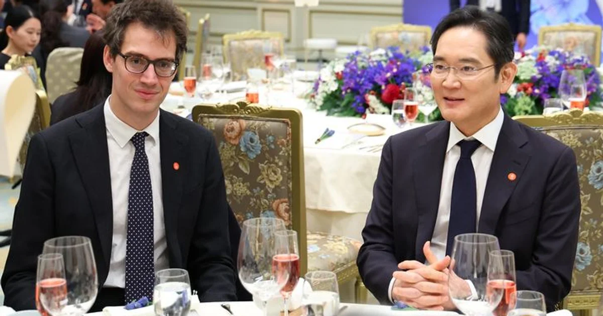
Samsung Electronics and Mistral AI announced their strategic partnership on September 9 during the South Korea-France state summit in Paris.
The collaboration is focused on Samsung's semiconductor operations. Mistral's software and models, including Mistral Large, will be adapted to engineering and manufacturing workloads rather than simply installed as another general-purpose corporate chatbot.
Samsung wants the models running inside its own infrastructure
The deployment will be on-premises. Samsung says sensitive operational and technology data can therefore remain within its semiconductor infrastructure while engineers use customized AI systems.
That distinction matters in chip manufacturing. Process recipes, defect information, equipment behavior and yield data can reveal details about technologies that semiconductor companies spend years and billions of dollars developing.
A public-cloud assistant is not an obvious place to send that information.
Mistral has made private and controllable enterprise deployments an important part of its commercial strategy, giving Samsung a way to use large models while retaining tighter control over the underlying data.
Defect detection is one of the first targets
Samsung specifically identifies defect detection and equipment optimization as workloads for the new systems.
A modern fab produces enormous quantities of process and metrology data. Finding useful correlations across those records can help engineers identify where a defect was introduced, which equipment behavior preceded it and whether similar patterns have appeared elsewhere.
Samsung also wants AI to accelerate development cycles and stabilize manufacturing yields more quickly.
Yield is where the economic argument becomes particularly important. A technically advanced process is far less valuable if too few working dies emerge from each wafer.
This is generative AI moving beyond office assistants
Enterprise AI adoption initially revolved around document summaries, coding assistants, search and writing tools. Semiconductor manufacturing gives large models a very different job.
An engineer could use a specialized system to navigate equipment documentation, compare defect histories, retrieve process information or narrow down relationships hidden inside large operational datasets.
That does not mean an LLM suddenly controls a fabrication line by itself.
Samsung has not published measured productivity or yield improvements from the partnership yet. The announcement describes where it intends to use the technology, not a completed autonomous-factory system.
Samsung is also putting money into Mistral
The relationship extends beyond software deployment. Samsung has taken a strategic equity position in Mistral as part of the French company's latest financing.
Mistral raised €3 billion in its Series D at a post-money valuation above €21 billion, a round the company describes as the largest equity fundraising ever completed by a private European technology company.
Samsung participated as one of the round's lead investors alongside the EQT-managed Scaleup Europe Fund and PSG Equity.
Neither Samsung nor Mistral disclosed Samsung's individual investment amount.
Mistral also gains a partner sitting at the center of AI hardware
The relationship is useful in the other direction. Training and serving large models requires accelerators, enormous memory bandwidth and increasingly specialized data-center infrastructure.
Samsung supplies DRAM, HBM, storage, logic manufacturing and advanced foundry and packaging services across that stack.
The companies had already been discussing cooperation earlier in 2026. Mistral CEO Arthur Mensch met Samsung semiconductor executives in Korea to discuss AI memory supply and related technologies.
Samsung is building a web of AI partnerships
Mistral is only one part of Samsung's broader AI strategy. The company already works with major infrastructure players including NVIDIA and OpenAI.
Its semiconductor division is shipping samples of 12-layer HBM4E while developing additional memory architectures for future AI accelerators.
Samsung has also expanded its relationship with ASML around High-NA EUV lithography and plans to introduce the technology into future high-volume DRAM manufacturing from 2028.
The pieces increasingly connect: Samsung builds hardware for AI systems, those systems generate tools that can improve semiconductor manufacturing, and the improved manufacturing process feeds the next generation of AI hardware.
The useful benchmark will be yield, not chatbot eloquence
A semiconductor fab is an unforgiving environment for probabilistic software. A plausible but incorrect answer can send an engineer toward the wrong diagnosis rather than merely producing a bad paragraph.
Mistral's models will therefore have to operate alongside validated industrial data, conventional analytics and human engineering controls.
The partnership becomes meaningful if Samsung eventually demonstrates shorter process-development cycles, earlier defect detection or faster yield stabilization.
That is a less glamorous benchmark than a new model leaderboard. For a chip manufacturer, it may be considerably more valuable.