
 By Adri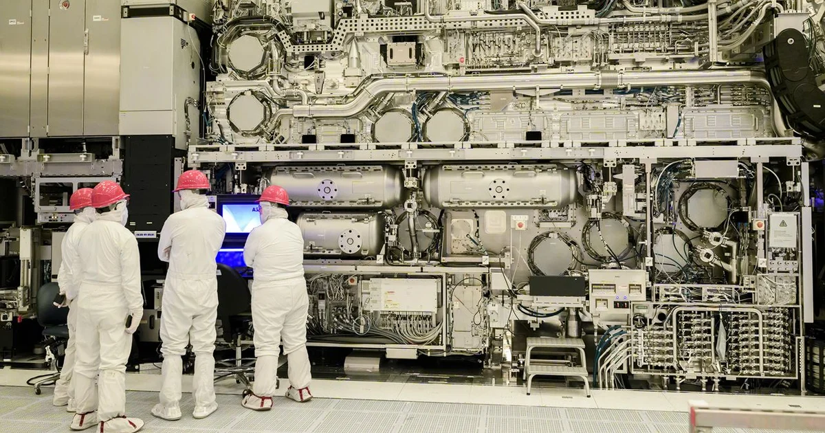
One million wafers does not mean one million Panther Lake wafers
There is an important qualifier behind the headline number. Intel and ASML's total combines early tool certification and testing, research and development work, and volume production. It should not be read as one million commercial Panther Lake wafers manufactured entirely with High-NA.
The production milestone itself is established. Intel uses ASML's EXE High-NA systems for selected layers on a subset of Core Ultra Series 3 processors. Those Intel 18A layers are dual-qualified in Oregon, allowing them to be patterned either with High-NA or conventional 0.33 NA NXE EUV equipment.
When ASML disclosed the production deployment in July, it said the High-NA option was shipping product at yields matched to the NXE platform. Intel's September update adds that overlay, throughput and availability are meeting its expectations.
The optical change is 0.33 to 0.55 NA
ASML's established NXE EUV systems operate at a numerical aperture of 0.33. The EXE platform increases that figure to 0.55, improving imaging resolution and allowing smaller features to be patterned without relying as heavily on multiple patterning steps.
When Intel completed installation of its first commercial EXE:5000 in 2024, it said High-NA could enable features up to 1.7 times smaller than existing EUV tools and as much as 2.9 times the two-dimensional feature density. Those are lithography capability figures, not a promise that a commercial processor automatically becomes 2.9 times denser.
Reducing patterning complexity is another part of the attraction. ASML designed the EXE platform to replace multiple exposures with single-exposure patterning for suitable critical layers. Fewer process steps can shorten manufacturing cycles while avoiding some of the alignment complexity introduced by multipatterning.
Intel 18A is already the production test bed
Intel originally framed High-NA primarily as part of its process roadmap beyond Intel 18A, including future Intel 14A manufacturing. It has now inserted the technology earlier as an optional production path for selected 18A layers.
Panther Lake should not consequently be described as an entirely High-NA-made processor. Intel explicitly limits the deployment to selected layers and a subset of Core Ultra Series 3 products. Keeping those layers qualified on both EXE and NXE tools also gives the foundry flexibility when allocating expensive lithography capacity.
The production run provides Intel and ASML with data before broader future insertion. Intel continues developing 14A, with multiple customers evaluating its PDKs and the company previously saying it expected early design commitments to begin emerging in the second half of 2026. Whether an individual future layer uses High-NA will still be a process decision rather than something guaranteed simply by the 14A name.
The next problem is the size of the mask
High-NA's larger numerical aperture comes with a smaller exposure field. Large dies can therefore require stitching, where separately exposed fields are joined with sufficient precision to behave as one design.
Intel and ASML say manufacturers can obtain High-NA benefits with today's six-inch mask format. Designs can be floor-planned within the available field or use Intel Foundry's stitching capabilities and PDK support.
The longer-term solution is a larger mask. Intel has backed that transition for years, while ASML is also working with TSMC and Samsung on a future 12-inch photomask ecosystem. The ASML-TSMC initiative targets a 12-inch mask pilot line in 2031 and system readiness for advanced-node production in 2033. Those are future targets; current High-NA manufacturing does not depend on waiting for the larger mask.
From EXE:5000 to EXE:5200B
Intel installed the first commercial TWINSCAN EXE:5000 in Oregon in 2024. The system weighs more than 150 metric tons, and transporting it involved more than 250 crates packed into 43 freight containers before 20 trucks carried the equipment to the site.
The newer EXE:5200B is aimed more directly at high-volume manufacturing requirements. Intel was the first chipmaker to install and pass acceptance testing on the second-generation system. At this stage, resolution is only part of the challenge: throughput, uptime, overlay accuracy and manufacturing cost determine whether better optics are actually useful inside a production fab.
Passing one million processed wafers does not mean High-NA has replaced conventional EUV. Intel is using both technologies and can select them layer by layer. What has changed is the nature of the discussion. High-NA is no longer merely a machine demonstrating tiny lines in a laboratory; Intel and ASML now have to optimize it as equipment expected to keep a production line running.